Sign In | Join Free | My burrillandco.com
Home > Impedance Control PCB >

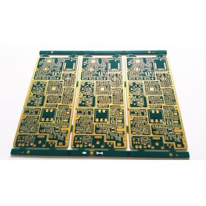
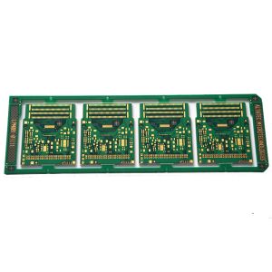
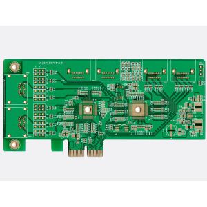
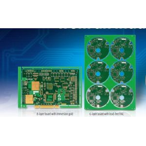
50 Ohm 4 Layer Impedance Control PCB With Hard Gold Fingers Green Soldermask

Global Success Circuits Co.,Ltd
Contact Now
    Buy cheap 50 Ohm 4 Layer Impedance Control PCB With Hard Gold Fingers Green Soldermask from wholesalers
     
    Buy cheap 50 Ohm 4 Layer Impedance Control PCB With Hard Gold Fingers Green Soldermask from wholesalers
    • Buy cheap 50 Ohm 4 Layer Impedance Control PCB With Hard Gold Fingers Green Soldermask from wholesalers

    50 Ohm 4 Layer Impedance Control PCB With Hard Gold Fingers Green Soldermask

    Ask Lasest Price
    Brand Name : Global Success Circuits
    Model Number : GPC63T15
    Certification : ISO9001: 2008,ISO TS16949: 2009 UL E324220
    Price :
    Payment Terms : L/C, D/A, D/P, T/T, Western Union
    Delivery Time : 5 - 15 days
    • Product Details
    • Company Profile

    50 Ohm 4 Layer Impedance Control PCB With Hard Gold Fingers Green Soldermask

    50 Ohm 4 Layer Impedance Control PCB With Hard Gold Fingers Green Soldermask


    PCB Features:


    • Layers: 4

    • Material: FR4 laminate, RoHS compliance

    • PCB thickness: 1.6mm ±10%

    • Final copper: 2/1/1/2oz

    • Minimum hole: 0.4mm

    • Minimum line width/space: 5/5-mil

    • Minimum hole copper: 25um

    • Solder mask: green

    • Legend: white

    • Surface finish: ENIG + gold fingers

    • Outline: rout and score

    • E-test: 100%

    • Inspection standard: IPC-A-600H/IPC-6012B, class 2/3

    • Outgoing reports: final inspection, first article report, E-test, solder ability test, micro section and more

    • Certificates: UL E324220, SGS, RoHS


    Our pcb capability


    Category

    Description

    Capability

    Laminate Material

    FR4, High TG FR4(tg150,tg170,tg180)
    Halogen-free FR4, CEM1, CEM3,Polyimide,
    Rogers ,Aluminum

    We will order other special material accoprding to your request

    Board Layers

    Maximum layers

    1-18layers

    Size

    Maximum finished dimensions

    500*1200mm

    Board Thickness

    Minimum and Maximum

    0.2-3.2mm

    Copper

    Outer copper weight

    0.5oz (17um) - 4oz (140um)

    Inner copper weight

    0.5oz (17um) - 4 oz (105um)

    Drilling

    Minimum drilling size

    0.15mm

    Drill Deviation (True position size)

    2mil (0.050mm)

    PTH hole tolerance

    3mil (0.075mm)

    N-PTH hole tolerance

    2mil (0.050mm)

    Minimum hole wall thickness

    20um

    Angle of Countersink

    80°, 90°, 100°, 120°

    Circuit line

    Minimum width

    0.1mm/ 4mil

    Minimum space

    0.1mm/ 4mil

    Inner Layers

    Minimum space from drilling to inner pattern

    6mil (0.15mm)

    Minimum space from annular ring to inner pattern

    6mil (0.15mm)

    Layer-to-layer registration

    3mil (0.08mm)

    Board Profilling

    Hole to board edge tolerance

    ±4mil (0.1mm)

    Pattern to board edge tolerance

    ±4mil (0.1mm)

    CNC Tolerance

    ±4mil (0.1mm)

    Minmum thickness after V-Cut

    12mil (0.3mm)

    V-Cut tolerance

    ±5mil (0.12mm)

    V-Cut Angle

    20,30,45,60

    Solder mask

    Color

    green, light green, matte green, white black,matte black,yellow,red, blue

    Thickness

    ≥17um

    Silkscreen

    Color

    White, black, yellow,
    red, blue, green, gray

    Minimum line height

    ≥0.0625mm

    Minimum line width

    ≥0.125mm

    Surface Finish

    HASL, HASL pb free, immersion gold, immersion silver, O.S.P

    Certification

    IPC-A-600 Class II/III, UL E324220, ISO 9001,ISO/TS16949, ROHS


    Product Structure


    SINGLE SIDED 15%


    DOUBLE SIDED 40%


    4-6 LAYERS 35%


    ≥8 LAYERS 10%


    Benefits of Double Sided PCBs:


    The multilayer PCB is the development of the double sided PCB. With increasing complexity and density of components many designers were struggling to find the route and size required for modern instruments. Adding just a power and ground plane to the inside of the board allowed the components to be powered with just two plated holes to the inner layers rather than a track back to a power/ground point. Once the technology to multilayer PCBs was established, it was further developed to have additional signal layers inside. This allowed the designers to produce highly complex and compact circuits and further development of blind and buried via hole technology has pushed these limits even further. The highly complex PCBs now being offered allow high density packaging to the designer’s requirement and in line with the most complex components.


    Main products


    Quality 50 Ohm 4 Layer Impedance Control PCB With Hard Gold Fingers Green Soldermask for sale
    Inquiry Cart 0
    Send your message to this supplier
     
    *From:
    *To: Global Success Circuits Co.,Ltd
    *Subject:
    *Message:
    Characters Remaining: (0/3000)